PCB Design
- 1. Capability & Strength
- 1. Comprehensive tester library and extensive experience in major test systems.
- 2. Impedance Controlled Product
- 3. High Speed - USB(2.0 / 3.0), MIPI, SATA
- 4. Design Guideline through previous simulations
- 2. Design Service
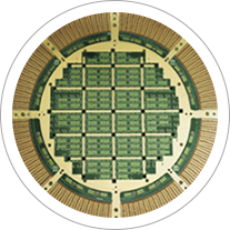
- 1. Probe Card (Cantilerver, Flipchip, WLCSP, VPC)
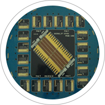
- 2. PIB, Loadboard, Direct Dock
- 3. Low Leakage Current PCB
- 4. Motherboards for PRVX
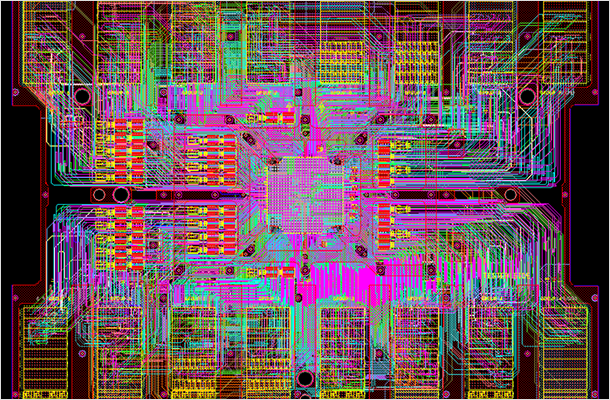
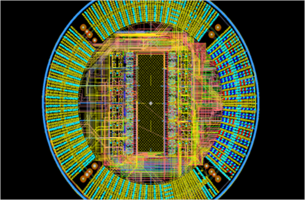
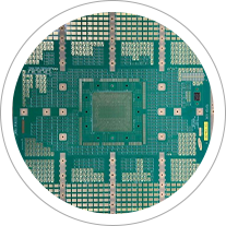
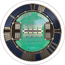
PCB Design Capabilities
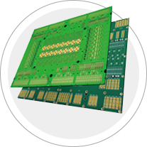
- Optimized PCB Design of Tester (ATE) for multi-layer production.
- As per customer’s request, Capabilities for PCB design and manufacturing including Digital, Analog, Mixed signal.
SOC (AP)
U-Flex (SD, XD, PLUS), T2000, V93K(DD) and etc.
Display Drive IC
T6371, T6372, T6373, T6391
TS7600, ST6730(A), Diamond X
MEMORY
T5830, T5377, T5833,
MT6121, DF8600, FOS8000,
V5400, K8000, Magnum5 (XV, SSV)
CIS
(Cmos Image Sensor)
IP750, IP750EX,
Magnum, T2000
PMIC
(Power Management IC)
ETS-600, T2000, U-Flex
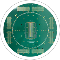
Load Board
V93K, T2000,
U-Flex, ETS364
PCB Manufacturing Capabilities
| ITEM | SPEC |
|---|---|
| Layer | ~140 Layers |
| Min, Pitch | 0.27 Pitch(Under 2T), 0.35 Pitch(Under 4.8T) |
| Option | BVH, HPL, Back-Drill, Build Up, BUMP |
| Imp Control | ±10% (DC resistor not included ±5%) |
| Finishes | ENIG, ELECTROLYTIC GOLD(Hard Gold) |
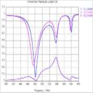
PCB Design for High speed signal processing
- Low DF (Dissipation Factor) material & Impedance matching (50, 90, 100Ω) design.
- Providing Simulation Data (SI/PI Software and engineer)
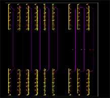
PCB Design
(Allegro)
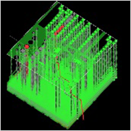
Modeling
(Power SI)
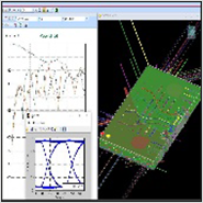
Simulation
(Power SI)
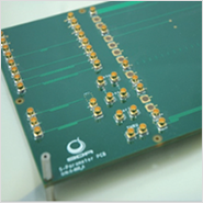
PCB
Sample Manufacturing

VNA measurement
(Anritsu MS46322A)
Consequences
& analysis
Delivery Management Process
- PCB designed by SDA, After manufacturing process, Quality inspection be conducted as well.
- In case Defective has been found during quality inspection, Repair & Modify service is provided by our C/S team.
-
AOI Inspection
(Automatic Optical Inspection)
-
BBT Test
(Bare Board Test)
-
1st Manual
(1st Manual Inspection)
-
2nd Manual Inspection
-
Component Test
-
Designer Confirm & Final Inspection
-
Delivery
