Laser Micro Hole Drilling SDL-FI200
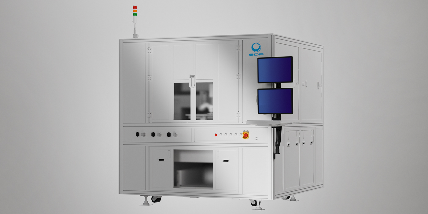
OUTLINE
- Vertical Probe card guide plate hole processing
- Hole processing according to Flexible probe pin shape
- Various types of material
(Ceramic, Polymers, Metal, Glass, etc.)
FEATURES
- High precision universal laser system (IR Pulsed Laser)
- High precision Scan System (Scan System Auto Calibration S/W)
- X,Y,Z,T Linear Motion System (2D Motion Auto Calibration S/W)
- Integrated Auto inspection Vision System
- Maximum hole processing size : 200mm × 200mm
- On The Fly Option
SPEC
| Si3N4 (Silicon Nitride) | 0.125 T | 0.25 T |
|---|---|---|
| Min. Hole Size | 30 × 30um | 30 × 30um |
| Min. Hole Pitch | > 40um | > 50um |
| Hole Taper | < 5um | < 10um |
| Corner Radius of Rectangular Hole | < R 4um | < R 6um |
| Hole Size Repeatability | ± 1.5um | ± 1.5um |
| Hole Position Error | ± 1.5um | ± 1.5um |
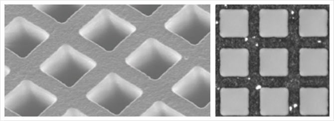
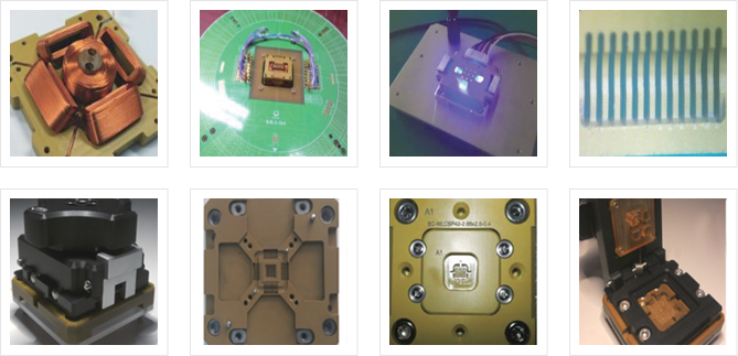
Micro Rectangular Holes on Guide Plates
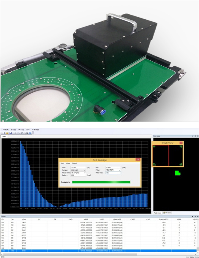
Low Leakage Tester
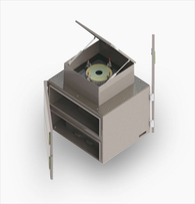
OUTLINE
- Probe card reliability verification equipment for DC parameter testing process
- To determine the interference between the channels of the probe card, measure the leakage current for each channel
SPEC
| ITEM | SPEC |
|---|---|
| Measuring Instruments | Keithley 6430 |
| Communication | RS232 |
| Number of Channel | 48CH. (Max : ~128CH) |
| Channel Board | 8CH. Per 1board |
| Measurement Range | 10aA ~ 105mA |
| Source Voltage | 0V~20V |
| Operating Environment | Temperature : 20℃(±1℃) Humidity : 30%~50% |
Relay Switching Board for Probe Card Tester
OUTLINE
- Probe Card Electrical Characterization Testing Equipment
- Replacement of mechanical relay channel control with electronic switch (MAX313L, Analog Switch)
- Guaranteed relay permanent lifespan, equipment miniaturization, and improved measurement speed
SPEC
| ITEM | SPEC |
|---|---|
| Measuring Instruments | Keithley 6487 Source Meter Agilent 4263B LCR Meter |
| Communication | RS485 |
| Number of Channel | ~ 5400CH |
| Channel Board | 100CH. per 1board |
| Source Voltage | 0V~20V |
| Operating Environment | Temperature : 20℃(±1℃) Humidity : 30%~50% |
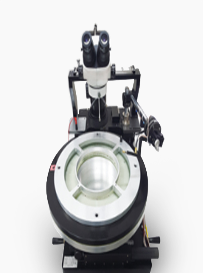
Probe Card Tester SDP3000
OUTLINE
- Probe Card Electrical Characterization Testing Equipment
- Capability to verify the X & Y positions and diameter of probe card tips
- Ability to test open and contact resistance of probe card tips
SPEC
| Item | SPEC | |
|---|---|---|
| Probe stage | x, y working area | 200X200mm |
| z axis working area: | 12mm | |
| z axis force | >100kg | |
| x, y, z precision | ±1um | |
| repeatability | ±1um | |
| Vision | F.O.V | X=0.86mm(SCAN) |
| working Distance | 20mm±2mm | |
| CCD | ½” | |
| resolution | 1600X1200 pixel | |
| Leakage Test | 1pA~2mA | |
PRVX Mother Board
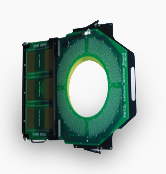
OUTLINE
- Motherboard used with probe card analysis equipment
- Components required for probe card correlation and performance measurement before production wafer testing
SPEC
| Layer | SPEC |
|---|---|
| Test Device | BGA, WLCSP, LED, ETC |
| Test Pitch (mm) | 0.35 / 0.4 / 0.5 / 0.65 / 0.75 / 0.8 / 1.0 |
| Temp | -50℃ ~ 200℃ |
| Life Cycles | > 300,000 Cycles |
| Test Pin | POGO Pin, J contactor |
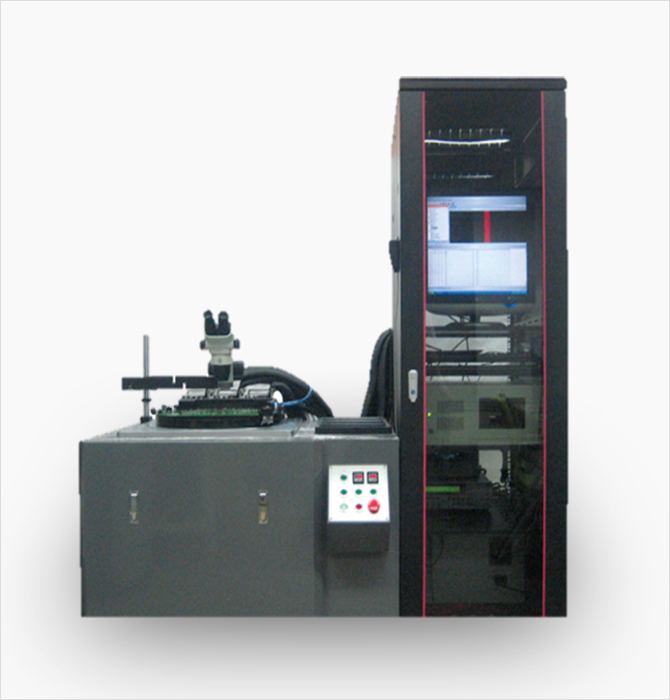
Probe Card Manual Tester SDP-200C
OUTLINE
- Manual inspection equipment for checking the connection between the probe pin and main PCB during the probe card manufacturing process
- Process equipment used to check the connection status of probe pins after probe card assembly or before shipment
SPEC
| ITEM | Contents |
|---|---|
| PC Specification | - CPU: Pentium
- OS: Windows 7 or higher - Monitor: 17” or larger - RAM: 2GB or more - Communication: RS232 |
| Equipment Size | 500mm × 1000mm × 550mm (excluding PC) |
| Equipment Weight | 30kg |
| Power | AC220V (60hz) |
| Current Consumption | 300mA or less |
Capability to manufacture various sockets for package verification
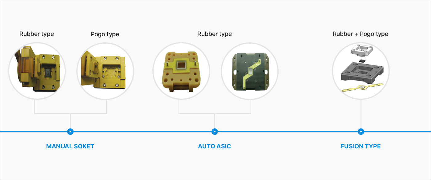
| ITEM | SPEC |
|---|---|
| Test device | BGA, WLCSP, LED, ETC |
| Test pitch[mm] | 0.35/0.4/0.5/0.65/0.75/0.8/1.0 |
| Temperature | -50℃ ~ 200℃ |
| Life cycle | > 300,000 Cycles |
| Test pin | POGO Pin, J contactor |
DMD Controller for Direct Image Exposer
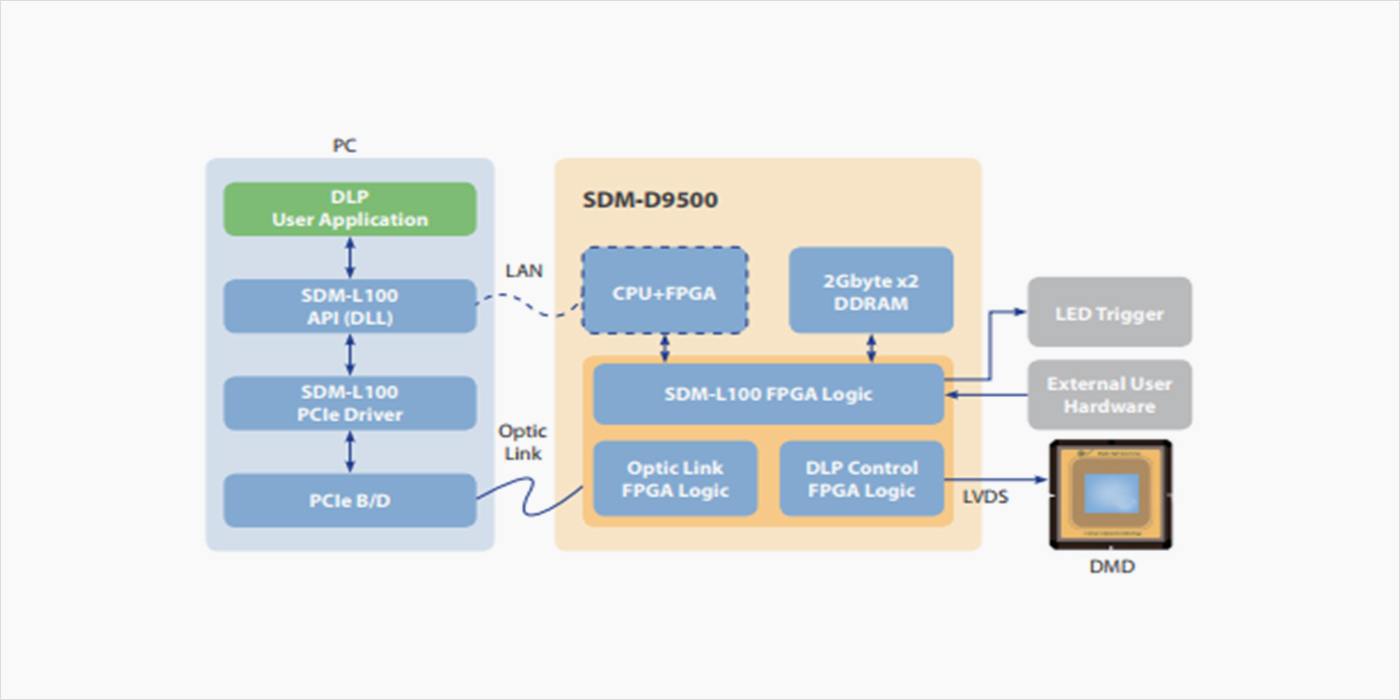
OUTLINE
- Controller for DLP 9500 Chip control
- Equipped with high-precision micro-pattern exposure algorithms
- Capable of development and production in OEM format
- Provides a rich software library optimized for image processing and exposure
SPEC
| ITEM | Common DMD Controller |
SDM-D9500 |
|---|---|---|
| DMD Tilting Angle | Fixed | Flexible |
| Exposer Resolution | Fixed | Flexible |
| Image Processing | S/W &H/W | S/W |
| FPGA Logic | H/W Dependent | H/W Independent |
FEATURE
-
Exposure method
-Application of DMD rotation and parallel exposure algorithms
- Various DMD tilt angles can be applied based on environment settings via software
-
Frame Per Sec
- 1920x1080 HD Binary Image at 16,000 FPS
- 1024x768 XGA Binary Image at 22,000 FPS
-
Brightness control
- Light intensity control via software
-
Image Format
- DXF File
- Gerber File
-
Main Feature
- No need for high-speed communication processing, reducing the controller size and hardware cost
- Adoption of an open hardware architecture, enabling the application of various applications
-
Power
- DC 12V, 8A
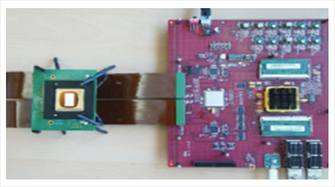
DMD Controller for Direct Image Exposer
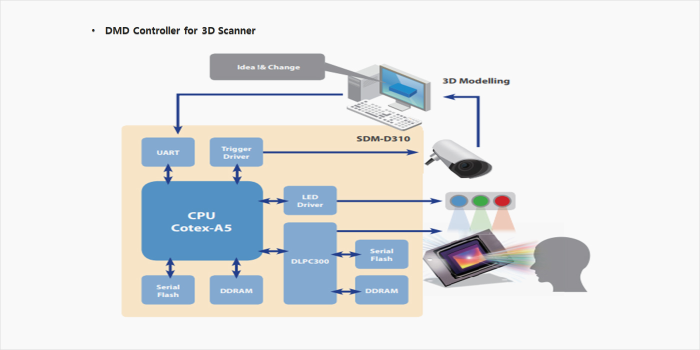
OUTLINE
- DMD Controller for compact 3D scanners
- Custom-made to optimize for the customer's system, with a provided software library
- Produced and supplied in OEM format
- Designed with only firmware and FPGA, ensuring hardware stability without using an OS kernel
FEATURE
-
Resolution
- 608 x 684
-
Frame Per Sec
- 360, 720, 960, 1440Hz (Max.4000Hz) @1bit
-
Number of patterns
- 20 Pattens
-
Image Format
- bitmap format
-
Interface
- UART
-
Electrical Characteristics
- Power Supply : DC 5V, 2A
- Operating Temperature : -20°C ~ 85°C
- Storage Temperature : -40°C ~ 85°C
- RGB LED Current : Min 300mA, Max 1.5A
